A single-phase semiconductor material, e.g., silicon and germanium, has intrinsic physical properties. When two semiconductor materials are joined to form “heterojunction” structures, special properties appear and can be used for applications in electronic, optoelectronic, and thermoelectric devices. To achieve ideal device performance, the heterojunction interface must be free of defects and possess compositional abruptness. Owing to recent advances in nanomaterial fabrication, defect-free heterojunction structures can be realized in nanowires. A nanowire is a one-dimensional structure with a diameter of less than 100 nanometers. When two sets of atoms with different periodicities are commensurately connected in a nanowire’s axial direction, the free surface of the nanowire sidewalls allows for atom displacement near the interface. The strain energy, which may cause interfacial defects, is reduced.
The method most routinely used for semiconductor nanowire growth includes a vapor-liquid-solid (VLS) mechanism. In this mechanism, semiconductor gas precursors are decomposed by liquid-phase catalysts, followed by precipitation of solid semiconductors at the liquid/solid interface. The nanoscale cross-sectional area of the liquid/solid interface allows the formation of one-dimensional nanowires via continuous precipitation. Nanowire heterojunctions are produced by simply switching the gas precursors during VLS growth. However, the commonly used liquid catalysts have a certain semiconductor material solubility, which limits prompt composition changes at the interface. In addition, the nanowire morphology usually changes after switching the gas precursors.
A new approach for forming heterojunctions in nanowires was recently found. [1] In this method, as-grown SiGe alloy (Ge concentration: 6%) nanowires are oxidized in air (at 700°C for 6 hours). After oxidization, an oxide shell surrounding the entire nanowire forms, and a heterojunction is also produced in the nanowire, as shown in Figure 1a. An interface between the original SiGe alloy and a Ge-rich section is also created. Interestingly, the heterojunction interface is atomically abrupt – the change in the Ge concentration across the interface is within one atomic plane, as shown in Figure 1b.
According to the phase diagram, the Au at the nanowire tip (Figure 1a) forms an AuGeSi liquid alloy during oxidation, and this liquid phase plays an important role in the formation of the heterojunction structure. Because Si is more easily oxidized than Ge, the Ge atoms are ejected from the oxide shell and diffuse to the liquid phase during the oxidation process. As a result, the relative concentration ratio of Ge to Si in the AuGeSi liquid increases. The sharp interface in Figure 1b implies that the Ge-rich section forms via layer-by-layer growth of SiGe atomic planes at the liquid/solid interface, which has been observed by in situ transmission electron microscopy (TEM) analysis. In this mechanism, the composition of each atomic layer is associated with the concentrations of Si and Ge in the AuGeSi liquid phase. Since the concentration ratio of Ge to Si in the AuGeSi liquid increases, the newly precipitated atomic layer has a higher Ge concentration, resulting in an abrupt change in the composition at the interface.
A compositionally abrupt interface is produced in SiGe alloy nanowires by a simple oxidation step. The sharp interface distinctly defines two sections with different physical properties, e.g., thermal conductivity. Additional interesting properties are expected to be found in other such heterojunction nanowire structures. The composition of the AuGeSi liquid can also be altered as a result of preferential Si oxidation. Precipitation from the AuGeSi liquid, which has an altered Ge to Si compositional ratio, creates a heterointerface with the parent SiGe phase. This process can be further applied for the fabrication of other SiGe heterojunction nanomaterials.
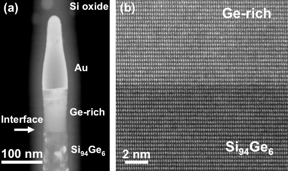
Figure 1. (a) Scanning transmission electron microscopy (STEM) image of a SiGe heterojunction nanowire produced by oxidation. The interface is labeled by an arrow. (b) STEM image of the interface between the original Si94Ge6 nanowire section and the Ge-rich section. In STEM mode, the image intensity contains chemical information. The heavier element produces a stronger image intensity; therefore, the sharp contrast change across the interface indicates an abrupt change in composition.
References
Lee, H., Shen, T., Hu, C., Tsai, Y., & Wen, C. (2017). Producing Atomically Abrupt Axial Heterojunctions in Silicon–Germanium Nanowires by Thermal Oxidation. Nano Letters, 17(12), 7494-7499. doi:10.1021/acs.nanolett.7b03420.
Cheng-Yen
Wen
Professor, Department of Materials Science and Engineering
cwen@ntu.edu.tw